Term of the Moment
desktop computer
Definition: angstrom era
The angstrom era refers to the precision in today's chip making machines that are able to align the next lithographic plate within one to two nanometers (10 to 20 angstroms) over the previous layer. We are definitely in the angstrom era.
Angstrom Branding Is Not Really in Angstroms
Since the beginning of processor manufacturing in the 1950s, the size of the elements in a transistor have been shrinking from as large as 120,000 nanometers to approximately 12 to 40 nm today. Starting in the 1990s, this "feature size" was turned into a brand, and every couple years, the number got smaller.
Angstroms Are In!
Absolute Angstrom Precision
Angstrom Branding Is Not Really in Angstroms
Since the beginning of processor manufacturing in the 1950s, the size of the elements in a transistor have been shrinking from as large as 120,000 nanometers to approximately 12 to 40 nm today. Starting in the 1990s, this "feature size" was turned into a brand, and every couple years, the number got smaller.
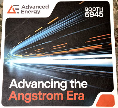
This banner was At the HumanX AI conference in Las Vegas in March 2025. Angstroms sound really high tech, and we are, in fact, in the angstrom era with regard to precision.
ASML's EUV machines are most definitely in the Angstrom era. The initial alignment between wafer and photomask (reticle) may be from one to three angstroms, and subsequent aligments between layers must be from one to two nanometers (10 to 20 angstroms). See EUV machine. (Image courtesy of ASML.)