AI Term of the Moment
AI power consumption
Definition: TSMC 3DFabric
TSMC's advanced packaging techniques for its state-of-the-art chips. In 2020, TSMC merged their 2.5D and 3D packages into the 3DFabric brand. Following are the various technologies.
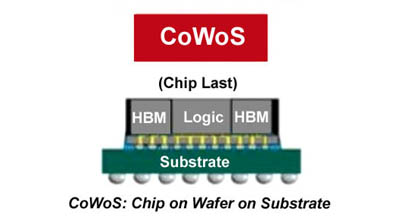
2.5D - Chip on Wafer on Substrate
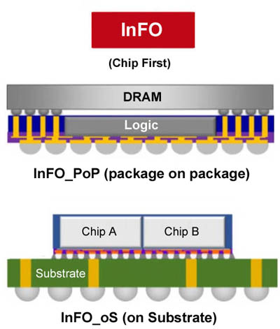
2.5D - Integrated Fan Out
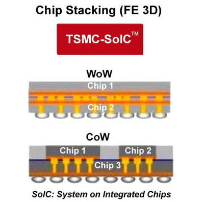
3D - Small Outline IC
This is the traditional chip-on-wafer method. CoWoS-R replaces the costly silicon interposer spanning the die with an organic substrate. CoWoS-L uses a "local" silicon bridge for very short interconnections between dies. Chip last means the die is attached after the electrical connections are made. (Image courtesy of TSMC.)
The InFO method adds the packaging directly on the wafer. It uses a high-density redistribution layer (RDL) for dense connections between chip and board, and InFO packages are thinner than traditional designs. Chip first means the dies are added before the electrical connections. (Images courtesy of TSMC.)
A much more advanced version than the traditional small outline IC (SOIC) package, TSMC's 3D SoIC stacks the chips either face to face or back to back. WoW is wafer-on-wafer, and CoW is chip-on-wafer. Through-silicon vias (TSVs) provide connectivity through the stack. See SOIC and via. (Images courtesy of TSMC.)